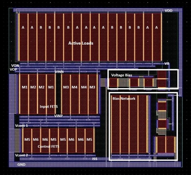
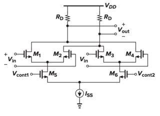
Current Bias Network, Active Loads, Differential Amplifiers, Voltage Bias Network, in one circuit.
Layout, extraction, then reitarate
Characterized, accounting channel length modulation, µCOX for NMOS and PMOS using SkyWater 130nm process technology, analyzed second-order effects such as velocity saturation and drain-induced barrier effects resulting from short-channel effects
Designed, simulated, and implemented a custom layout using design rule checks (DRC) and layout versus schematic (LVS) for the current bias network, differential and transconductance amplifiers, extracted and reiterated accounting parasitics
Tested various DC bias points (Q-point), saturation voltages, and width/length of FETs for the desired gain and output swing for a Variable Gain Amplifier (VGA); designed, extracted, and reiterated the layout accounting for process variation and parasitics
Simulated various control voltage and input voltage ranges including back-gate effects, ensuring the proper region of operation of all FETs and designed a DC bias voltage network for the active load in the amplifier